Semiconductor Materials
A semiconductor is a substance, usually a solid chemical element or compound, that can conduct electricity under some conditions but not others, making it a good medium for the control of electrical current. Its conductance varies depending on the current or voltage applied to a control electrode, or on the intensity of irradiation by infrared (IR), visible light, ultraviolet (UV), or X rays. The specific properties of a semiconductor depend on the impurities, or dopants, added to it. An N-type semiconductor carries current mainly in the form of negatively-charged electron.
A chip, an LED and a transistor are all made from semiconductor material.
Elemental semiconductors include antimony, arsenic, boron, carbon, germanium, selenium, silicon, sulfur, and tellurium. Silicon is the best-known of these, forming the basis of most integrated circuits (ICs). Common semiconductor compounds include gallium arsenide, indium antimonide, and the oxides of most metals. Of these, gallium arsenide (GaAs) is widely used in low-noise, high-gain, weak-signal amplifying devices.
 “Chip” Semiconductor from Texas Instruments.
A semiconductor device can perform the function of a vacuum tube having hundreds of times its volume. A single integrated circuit (IC), such as a microprocessor chip, can do the work of a set of vacuum tubes that would fill a large building and require its own electric generating plant. Semiconductors have had a monumental impact on our society.
You find semiconductors at the heart of microprocessor chips as well as transistors. Anything that’s computerized or uses radio waves depends on semiconductors. Today, most semiconductor chips and transistors are created with silicon. You may have heard expressions like “Silicon Valley” and the “silicon economy,” and that’s why — silicon is the heart of any electronic device.
 Silicon Valley
Today, most semiconductor chips and transistors are created with silicon. You may have heard expressions like “Silicon Valley” and the “silicon economy,” and that’s why — silicon is the heart of any electronic device. A diode is the simplest possible semiconductor device, and is therefore an excellent beginning point if you want to understand how semiconductors work. In this article, you’ll learn what a semiconductor is, how doping works and how a diode can be created using semiconductors. But first, let’s take a close look at silicon. Silicon is a very common element — for example, it is the main element in sand and quartz. If you look “silicon” up in the periodic table, you will find that it sits next to aluminum, below carbon and above germanium.
 Silicon sits next to aluminum and below carbon in the periodic table.
Carbon, silicon and germanium (germanium, like silicon, is also a semiconductor) have a unique property in their electron structure — each has four electrons in its outer orbital. This allows them to form nice crystals. The four electrons form perfect covalent bonds with four neighboring atoms, creating a lattice. In carbon, we know the crystalline form as diamond. In silicon, the crystalline form is a silvery, metallic-looking substance.
 In a silicon lattice, all silicon atoms bond perfectly to four neighbors, leaving no free electrons to conduct electric current. This makes a silicon crystal an insulator rather than a conductor.
Metals tend to be good conductors of electricity because they usually have “free electrons” that can move easily between atoms, and electricity involves the flow of electrons. While silicon crystals look metallic, they are not, in fact, metals. All of the outer electrons in a silicon crystal are involved in perfect covalent bonds, so they can’t move around. A pure silicon crystal is nearly an insulator — very little electricity will flow through it.
 Semiconductor band structure.
In solid state physics (and related applied fields), the band gap is the energy difference between the top of the valence band and the bottom of the conduction band in insulators and semiconductors. It is often spelt “bandgap“.
The band gap of a semiconductor
The band gap of a semiconductor is important for a number of reasons. An intrinsic (pure) semiconductor’s conductivity is strongly dependent on the band gap. This is because the only available carriers for conduction are the electrons which manage to get enough thermal energy to be excited from the valence band into the conduction band. From Fermi-Dirac statistics, the probability of these excitations occurring is proportional to:
where:
exp is the exponential function
Eg is the band gap energy
k is Boltzmann’s constant
T is temperature
 The Closed Semiconductor Design
In many devices this kind of conductivity is undesirable, and larger bandgap materials give better performance. In infrared photodiodes, a small band gap semiconductor is used to allow detection of low-energy photons. The ability to tailor the bandgap of a device is possible in semiconductor alloys (such as GaAlAs, InGaAs, InAlAs, etc…), and is sometimes referred to as bandgap engineering. This is exploited in the design of heterojunction bipolar transistors (HBTs) and laser diodes.
The difference between semiconductors and insulators is rather ambiguous. Indeed, according to one definition, a semiconductor is a type of insulator. In general, a material with a sufficiently large band gap will be an insulator. The figure of 3 eV is sometimes given. Mobility also plays a role in determining a material’s informal classification. Band gap decreases with increasing temperature, in a process related to thermal expansion. Bandgaps can be either direct or indirect bandgaps.
 In a single H-atom an electron resides in well known orbitals. Note that the orbitals are called s,p,d in order of increasing circular current.
A semiconductor is a material with electrical conductivity due to electron flow (as opposed to ionic conductivity) intermediate in magnitude between that of a conductor and an insulator. This means a conductivity roughly in the range of 103 to 10?8 siemens per centimeter. Semiconductor materials are the foundation of modern electronics, including radio, computers, telephones, and many other devices. Such devices include transistors, solar cells, many kinds of diodes including the light-emitting diode, the silicon controlled rectifier, and digital and analog integrated circuits. Similarly, semiconductor solar photovoltaic panels directly convert light energy into electrical energy. In a metallic conductor, current is carried by the flow of electrons. In semiconductors, current is often schematized as being carried either by the flow of electrons or by the flow of positively charged “holes” in the electron structure of the material. Actually, however, in both cases only electron movements are involved.
 Semiconductor Wafer Manufacturing
Silicon is used to create most semiconductors commercially. Dozens of other materials are used, including germanium, gallium arsenide, and silicon carbide. A pure semiconductor is often called an “intrinsic” semiconductor. The electronic properties and the conductivity of a semiconductor can be changed in a controlled manner by adding very small quantities of other elements, called “dopants”, to the intrinsic material. In crystalline silicon typically this is achieved by adding impurities of boron or phosphorus to the melt and then allowing the melt to solidify into the crystal. This process is called “doping”.
 Doping Semiconductor
The property of semiconductors that makes them most useful for constructing electronic devices is that their conductivity may easily be modified by introducing impurities into their crystal lattice. The process of adding controlled impurities to a semiconductor is known as doping. The amount of impurity, or dopant, added to an intrinsic (pure) semiconductor varies its level of conductivity. Doped semiconductors are often referred to as extrinsic. By adding impurity to pure semiconductors, the electrical conductivity may be varied not only by the number of impurity atoms but also, by the type of impurity atom and the changes may be thousand folds and million folds. For example, 1 cm3 of a metal or semiconductor specimen has a number of atoms on the order of 1022. Since every atom in metal donates at least one free electron for conduction in metal, 1 cm3 of metal contains free electrons on the order of 1022. At the temperature close to 20 °C , 1 cm3 of pure germanium contains about 4.2×10²² atoms and 2.5×10¹³ free electrons and 2.5×10¹³ holes (empty spaces in crystal lattice having positive charge) The addition of 0.001% of arsenic (an impurity) donates an extra 1017 free electrons in the same volume and the electrical conductivity increases about 10,000 times.”
 n-doping with phosphorus
The materials chosen as suitable dopants depend on the atomic properties of both the dopant and the material to be doped. In general, dopants that produce the desired controlled changes are classified as either electron acceptors or donors. A donor atom that activates (that is, becomes incorporated into the crystal lattice) donates weakly bound valence electrons to the material, creating excess negative charge carriers.

These weakly bound electrons can move about in the crystal lattice relatively freely and can facilitate conduction in the presence of an electric field. (The donor atoms introduce some states under, but very close to the conduction band edge. Electrons at these states can be easily excited to the conduction band, becoming free electrons, at room temperature.) Conversely, an activated acceptor produces a hole. Semiconductors doped with donor impurities are called n-type, while those doped with acceptor impurities are known as p-type. The n and p type designations indicate which charge carrier acts as the material’s majority carrier. The opposite carrier is called the minority carrier, which exists due to thermal excitation at a much lower concentration compared to the majority carrier.
p-doping with boron
The concept of holes can also be applied to metals, where the Fermi level lies within the conduction band. With most metals the Hall effect indicates electrons are the charge carriers. However, some metals have a mostly filled conduction band. In these, the Hall effect reveals positive charge carriers, which are not the ion-cores, but holes. In the case of a metal, only a small amount of energy is needed for the electrons to find other unoccupied states to move into, and hence for current to flow. Sometimes even in this case it may be said that a hole was left behind, to explain why the electron does not fall back to lower energies. It cannot find a hole. In the end in both materials electron-phonon scattering and defects are the dominant causes for resistance.
 Fermi-Dirac distribution. States with energy ? below the Fermi energy, here µ, have higher probability n to be occupied, and those above are less likely to be occupied. Smearing of the distribution increases with temperature.
The energy distribution of the electrons determines which of the states are filled and which are empty. This distribution is described by Fermi-Dirac statistics. The distribution is characterized by the temperature of the electrons, and the Fermi energy or Fermi level. Under absolute zero conditions the Fermi energy can be thought of as the energy up to which available electron states are occupied. At higher temperatures, the Fermi energy is the energy at which the probability of a state being occupied has fallen to 0.5. The dependence of the electron energy distribution on temperature also explains why the conductivity of a semiconductor has a strong temperature dependency, as a semiconductor operating at lower temperatures will have fewer available free electrons and holes able to do the work.

Worldwide semiconductor revenue totaled $270.3 billion in 2007, a 2.9 percent increase from 2006, according to preliminary results from Gartner. Vendor performances were mixed with two vendors in the top 10 that experienced double-digit growth and two vendors that showed declines in revenue. While the global market for dynamic random-access memory (DRAM) is expected to decline in 2007 due to a severe drop in prices caused by oversupply, Samsung Electronics is expected to increase its revenue by slightly higher than the overall global semiconductor market growth rate (DRAM is one the firm’s main products). Its growth is driven by steady revenue growth in NAND Flash Memory and strong revenue growth in nonmemory areas such as application processors, media integrated circuits (IC), complementary metal-oxide semiconductor (CMOS) image sensor, smart card ICs and LCD driver ICs.
You might also like
Random Posts
- Aluminum alloy
Aluminum is a very versatile metal and can be cast in any form known. It can be rolled, stamped, drawn, spun, roll-forme... - Titanium and It’s Alloys
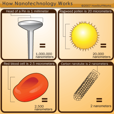
Titanium was discovered in Cornwall, England, by William Gregor in 1791 and named by Martin Heinrich Klaproth for the Ti... - What is Nanotechnology?
Nanotechnology is the engineering method in which fully functioning devices are manufactured at the molecular scale. ... - Heat Treatment of Steel
Heat treating is a group of industrial and metalworking processes used to alter the physical, and sometimes chemical, pr... - Characterization of Materials
Characterization, when used in materials science, refers to the use of external techniques to probe into the internal st...
© Copyright. Metallurgy for Dummies. All Rights Reserved.
Terms |
Site Map


 Alloy Suppliers
  Aluminum
  Aluminum Extrusions
  Copper-Brass-Bronze
  Nickel
  Magnets
  Stainless Steel
  Stainless Steel Tubing
  Steel Service Centers
  Titanium
  Tungsten
  Wire Rope