Nanoelectronics refer to the use of nanotechnology on electronic components, especially transistors. Although the term nanotechnology is generally defined asutilizing technology less than 100 nm in size, nanoelectronics often refer to transistor devices that are so small that inter-atomic interactions and quantum mechanical properties need to be studied extensively. As a result, present transistors do not fall under this category, even though these devices are manufactured with 45 nm, 32 nm, or 22 nm technology.
 Nanoelectronics refer to the use of nanotechnology on electronic components
In 1965 Gordon Moore observed that silicon transistors were undergoing a continual process of scaling downward, an observation which was later codified as Moore’s law. Since his observation transistor minimum feature sizes have decreased from 10 micrometers to the 28-22 nm range in 2011. The field of nanoelectronics aims to enable the continued realization of this law by using new methods and materials to build electronic devices with feature sizes on the nanoscale.
The volume of an object decreases as the third power of its linear dimensions, but the surface area only decreases as its second power. This somewhat subtle and unavoidable principle has huge ramifications. For a normal-sized drill, the power of the device is enough to handily overcome any friction. However, scaling its length down by a factor of 1000, for example, decreases its power by 10003 (a factor of a billion) while reducing the friction by only 10002 (a factor of “only” a million). Proportionally it has 1000 times less power per unit friction than the original drill. If the original friction-to-power ratio was, say, 1%, that implies the smaller drill will have 10 times as much friction as power.
These schematics illustrate the ‘vertical’ and ‘angled’ molecular junction configurations for mechanically-induced switching. A study has revealed that electrical resistance through such a junction can be turned ‘on’ and ‘off’ simply by pushing (left) so that the configuration is vertical or and by pulling the junction so that the configuation is angled. (Credit: Image courtesy of DOE/Lawrence Berkeley National Laboratory)
For this reason, while super-miniature electronic integrated circuits are fully functional, the same technology cannot be used to make working mechanical devices beyond the scales where frictional forces start to exceed the available power. The above being said, molecular evolution has resulted in working cilia, flagella, muscle fibers and rotary motors in aqueous environments, all on the nanoscale. These machines exploit the increased frictional forces found at the micro or nanoscale. Unlike a paddle or a propeller which depends on normal frictional forces (the frictional forces perpendicular to the surface) to achieve propulsion, cilia develop motion from the exaggerated drag or laminar forces (frictional forces parallel to the surface) present at micro and nano dimensions. To build meaningful “machines” at the nanoscale, the relevant forces need to be considered.
The global market for nano-electronics worth hundreds of billions of euros and this industry is the driving force behind the development of nanotechnology today.
We are faced with the development and design of intrinsically pertinent machines rather than the simple reproductions of macroscopic ones. For example, single electron transistors, which involve transistor operation based on a single electron. Nanoelectromechanical systems also fall under this category. Nanofabrication can be used to construct ultradense parallel arrays of nanowires, as an alternative to synthesizing nanowires individually. Besides being small and allowing more transistors to be packed into a single chip, the uniform and symmetrical structure of nanotubes allows a higher electron mobility (faster electron movement in the material), a higher dielectric constant (faster frequency), and a symmetrical electron/hole characteristic
The aim of Nanoelectronics is to process, transmit and store information by taking advantage of properties of matter that are distinctly different from macroscopic properties. The relevant length scale depends on the phenomena investigated: it is a few nm for molecules that act like transistors or memory devices, can be 999 nm for quantum dot where the spin of the electron is being used to process information. Microelectronics, even if the gate size of the transistor is 50 nm, is not an implementation of nanoelectronics, as no new qualitative physical property related to reduction in size are being exploited.
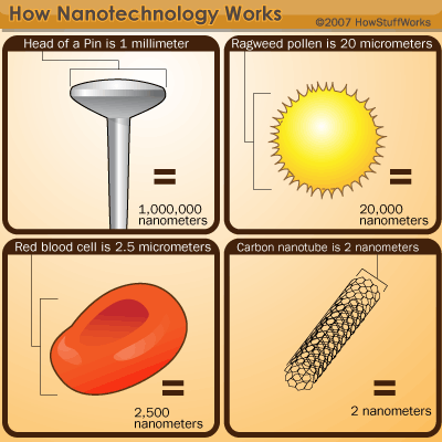
The smallest thing your eye can see might be a silk fibre. Imagine something thousand times smaller and you have reached the mysterious realm of the “nanoworld” where billions of electronic devices can be produced in the space of just a few square millimetres.
Single molecule devices are another possibility. These schemes would make heavy use of molecular self-assembly, designing the device components to construct a larger structure or even a complete system on their own. This can be very useful for reconfigurable computing, and may even completely replace present FPGA technology.
Semiconductor electronics have seen a sustained exponential decrease in size and cost and a similar increase in performance and level of integration over the last thirty years (known as Moore’s Law). The latter is a direct consequence of the shrinking device size, leading to physical phenomena impeding the operation of current devices. Quantum and coherence effects, high electric fields creating avalanche dielectric breakdowns, heat dissipation problems in closely packed structures as well as the non-uniformity of dopant atoms and the relevance of single atom defects are all roadblocks along the current road of miniaturization.
The flexible wireless monitoring system for vital body parameters with embedded microcontroller chip.
These phenomena are characteristic for structures a few nanometers in size and, instead of being viewed as an obstacle to future progress might form the basis of post-silicon information processing technologies. Specifically, by electronics we mean the handling of complicated electrical wave forms for communicating information as in cellular phones, probing and data processing as in computers. Concepts at the fundamental research level are being persued world-wide to find nano-solutions to these three characteristic applications of electronics.
Nanoelectronics holds some answers for how we might increase the capabilities of electronics devices while we reduce their weight and power consumption. Molecular electronics is a new technology which is still in its infancy, but also brings hope for truly atomic scale electronic systems in the future. One of the more promising applications of molecular electronics was proposed by the IBM researcher Ari Aviram and the theoretical chemist Mark Ratner in their 1974 and 1988 papers Molecules for Memory, Logic and Amplification, (see Unimolecular rectifier). A model system was proposed with a spiro carbon structure giving a molecular diode about half a nanometre across which could be connected by polythiophene molecular wires.
Research is ongoing to use nanowires and other nanostructured materials with the hope to create cheaper and more efficient solar cells than are possible with conventional planar silicon solar cells. There is also research into energy production for devices that would operate in vivo, called bio-nano generators. A bio-nano generator is a nanoscale electrochemical device, like a fuel cell or galvanic cell, but drawing power from blood glucose in a living body, much the same as how the body generates energy fromfood.
The average person’s body could, theoretically, generate 100 watts ofelectricity (about 2000 food calories per day) using a bio-nano generator. The electricity generated by such a device could power devices embedded in the body (such as pacemakers), or sugar-fed nanorobots. Much of the research done on bio-nano generators is still experimental, with Panasonic’s Nanotechnology Research Laboratory among those at the forefront.
You might also like
 |
 |
 |
 |
 Alloy Suppliers
 Aluminum
 Aluminum Extrusions
 Copper-Brass-Bronze
 Nickel
 Magnets
 Stainless Steel
 Stainless Steel Tubing
 Steel Service Centers
 Titanium
 Tungsten
 Wire Rope